Monday 19 September 2011

Safety Sells: product stewardship and sustainability for nanotechnology

NovioNano® is the trusted provider of safety solutions for all nanotechnologies and its products.


Being at the forefront of nanosafety since 2006, we aid companies to gain maximum understanding on safety of their nanoproducts - during manufacturing as well as in-use. No matter if you are a nanotechnologies producer, a user or both, we have all the tools to support your business.

Safety is regarded too often as a burdensome nuisance and a money guzzler. An opinion that couldn’t be more wrong. Safety is a top-priority for consumers and, as a consequence, safety facts are a means to create value. Also, companies with high standards in occupational safety and product safety perform better1.

As an important building block for your business development, product stewardship and sustainability for nanotechnology products can be evaluated by Novionano ® for their safety. In this month’s newsflash, we feature our state of the art occupational safety package. What can we do for you to determine the occupational safety of your nanoproduct offerings?

Novionano® offers a comprehensive nano safety management package based on real data. This includes:

1) Inventory of nanomaterials (optional: assessment of Safety Data Sheets)
2) Identification of emission sources of nano-sized particles and aerosols from lab
scale to industrial production (Figure 1)
3) Exposure measurements (PIMEX Movie)
4) Sampling and offline analysis of emitted materials in our nanolab
5) Interpretation and advise according to current recommendations by OECD, ISO,
EPA, ASTM 2, including training


Fig 1. State of the art nano-particles measurement equipment, the Philips Aerasense NanoTracer® which determines particle numbers and diameters ranging from 10-300 nanometer.


PIMEX, PIcture Mix Exposure

The main idea of this unique combination of real time video and simultaneous NanoTracer® measurements, is to make invisible hazards in the work environment like exposure to dangerous chemicals, nanoparticles, physical load and noise, visible and in this manner facilitate the reduction of hazards in workplaces.


References:
1 Harvard Business Review. DOI : 10.1225/692042
2 OECD: Organisation for Economic Co-operation and Development; ISO:International Organization for Standardization; EPA: Environmental Protection Agency USA; ASTM:formerly known as American Society for Testing and Materials

Contact:

NovioNano | Ferdy Bremmer | T: +31 (0) 652637511 | E: info@novionano.com


Don’t miss next month’s NovioNano® news feature which will be on the topic of “Product Perfection": a focus on physical-chemical characterization and toxicity testing of nanoproducts.

Saturday 17 September 2011

Graphene Overtaking Carbon Nanotubes


By Cathleen Thiele, Technology Analyst, IDTechEx www.IDTechEx.com/nano 


Graphene Overtaking Carbon Nanotubes

Carbon Nanotubes (CNTs) have not yet met commercial expectations from a decade ago, and now hot on its heels is graphene. Graphene is considered a hot candidate for applications such as computers, displays, photovoltaics, and flexible electronics.

IDTechEx market forecasts indicate that CNT and graphene transistors may be commercially available in volume from 2015 onwards, according to the new report “Carbon Nanotubes and Graphene for Electronics Applications 2011-2021” www.IDTechEx.com/nano.
  
According to IDTechEx, the biggest opportunity for both materials is in printed and potentially printed electronics, where the value of these devices that partly incorporate these materials will reach over $44 billion in 2021.

In a comparably short time a large amount of graphene materials have become commercially available contributing to further advancements and application development. Potentially at a fraction of the cost of CNTs, graphene may displace carbon nanotubes and even Indium Tin Oxide (ITO) in some applications.

Displays and PV are Key Drivers
Flexible, see-through displays may be the one application that finally puts graphene into the commercial spotlight. Combined with other flexible, transparent electronic components being developed at Rice University and elsewhere, the breakthrough could lead to computers and solar cells that wrap around just about anything. IDTechEx predicts a market volume of over $25 billion in 2021 for OLED displays and PV alone, some of which will use graphene.

Graphene and its compounds are increasingly used to make transistors that show extremely good performance - a progress that comes with new cheaper production processes for the raw material. Transistors on the basis of graphene are considered to be potential successors for the some silicon components currently in use. Due to the fact that an electron can move faster through graphene than through silicon, the material shows potential to enable terahertz computing.

Promise for CNTs
On the other hand, carbon nanotubes are still a strong focus of research. They too are used for making transistors and are applied as conductive layers for the rapidly growing touch screen market. Still considered a viable replacement for ITO transparent conductors in some applications, CNTs are not out of the game yet. While the cost of carbon nanotubes was once prohibitive, it has been coming down in recent years as chemical companies build up manufacturing capacity.

  
Challenges
However, there are still hurdles to overcome on both sides. For carbon nanotubes these are especially related to the separation issue and consistent growth. Without the latter, carbon nanotubes will probably never be used for high-volume electronic applications. Graphene, on the other hand, lacks the ability to act as a switch because it has no band gap. However, recent activities of several academic institutions show promise that this restraining issue will soon be solved.

Printed Electronics Market
Nevertheless, a very important result from both sides for the printed electronics market are printable CNT inks and graphene-based inks that are beginning to hit the market. Learn more about the CNT & Graphene market in the latest IDTechEx report on the topic www.IDTechEx.com/nano.

The upcoming Printed Electronics & Photovoltaics USA conference & exhibition, which will take place in Santa Clara on November 30 and December 1, will cover all this and more in great detail www.IDTechEx.com/peUSA.


Graphene
Dr Narayan Hosmane from Northern Illinois University will tell us how he almost by accident produced high-yields of graphene instead of the expected single-wall carbon nanotubes by using the Dry-Ice Method. Synthetic methodologies for producing graphene on large quantities will be the topic of his presentation.

On the applications side, Kate Duncan from CERDEC, the U.S. Army Communications-Electronics Research, Development and Engineering Center, will go into detail about direct write approaches to nanoscale electronics.

Polymer solar cells have made significant progress in the past few years. Prof Yang Yang, head of the Yang Group at University of California, Los Angeles (UCLA), will give a brief summary on the state-of-the-art status on this and UCLA developments with G-CNTs, a hybrid graphene-carbon nanotube material.

US company Vorbeck Materials Inc. says that products using their patented graphene based electronic ink will appear in major retail stores sometime this year. Dr Sanjay Monie, Technology Development Manager, will give the latest R&D news on the Vor-ink™ line of conductive inks and coatings for the printed electronics industry, the world's first graphene-based commercial products.

Carbon Nanotubes
Stephen Turner, Brewer Science, will talk about Aromatic Hydrocarbon Functionalization of carbon nanotubes for conductive applications, “a new functionalization path that affords high concentration dispersions without destroying the electronic properties of the nanotube,“ as he puts it. CNTRENE® carbon nanotube solutions is only one of the innovative materials developed at Brewer Science for applications in semiconductors, advanced packaging/3-D ICs, MEMS, displays, LEDs, and printed electronics.

And of course, applications of carbon nanotubes will be among the topics:
Only recently, SouthWest Nanotechnologies (SWeNT) received a two-year, $500,000 Oklahoma Research Grant to commercialize printed TFTs using semiconducting inks, based on its single-wall carbon nanotube (SWCNT) technology in collaboration with Panasonic Boston Lab (PBL). Dr Philip Wallis, Director of Operations at SWeNT, the leading SWCNT producer in the U.S., will tell us more about their proprietary V2V™ ink technology and how they fabricate and test the TFT devices to assure the necessary performance is demonstrated.

And last, but not least, CNT field emission will be the topic of Dr Jamie Nova’s talk, Director of Operations at Applied Nanotech (ANI). The company offers a wide range of other metallic inks and pastes. At the 2010 show Applied Nanotech announced the introduction of one of the most suitable potential replacements for coated substrates - EXCLUCENT™, substrates on flexible transparent PET utilizing copper-based metallic mesh.

Printed Electronics USA 2011 will take place from November 30 to December 1, with Masterclasses being held on November 29 and December 2 at the Convention Center in Santa Clara, California. In addition, tours to local centers of excellence have been arranged, giving delegates a chance to see products and operations first hand. For full details, visit www.IDTechEx.com/peUSA

For more information on the topic please contact the author Cathleen Thiele at c.thiele@IDTechEx.com or to find out more about the Printed Electronics USA 2011 conference please contact the Event Manager Mrs. Chris Clare at c.clare@IDTechEx.com.

IDTechEx Dates:

RFID Europe 2011 | 27-28 September 2011 | Cambridge, UK
Energy Harvesting & Storage USA 2011 | 15-16 November | Boston, USA
Wireless Sensor Networks & RTLS USA 2011 | 15-16 November | Boston, USA
Printed Electronics & Photovoltaics USA 2011 | November 30 – December 1 | Santa Clara, CA, USA
Electric Vehicles: Land, Sea, Air USA 2012 | March 27-28, 2012 | San Jose, CA, USA


Widening Government Support for Printed Electronics

By Dr Peter Harrop, Chairman, IDTechEx

This year, the world's largest event on printed electronics, "printed Electronics USA" will reflect the widening government support for printed electronics. Beyond the burgeoning programs at universities and government research centers, this is particularly evident in military and electric vehicle work. The US Army reflects this in two presentations. One is an overview of materials printing capabilities and prototype development for US Army applications and the other concerns direct write approaches to nanoscale electronics.

Nowhere is the increased government support more in evidence than with electric vehicles by land, water and air, however. Governments and industry have committed $60 billion to electric vehicle programs in the last two years. New initiatives keep being announced for both hybrid and pure electric vehicles since, for unmanned aircraft, underwater and indoor vehicles we are in the age of the pure electric vehicle but for on and off-road vehicles, seagoing craft  and manned aircraft we are in the age of the hybrid electric vehicle.

For example, US Energy Secretary Steven Chu recently announced more than $175 million over the next three to five years to accelerate the development and deployment of advanced vehicle technologies. The funding will support 40 projects across 15 states and will help improve the fuel efficiency of next generation vehicles. The projects will target new innovations throughout the vehicle, including better fuels and lubricants, lighter weight materials, longer-lasting and cheaper electric vehicle batteries and components, more efficient engine technologies, and more. This comprehensive approach to vehicle efficiency research and development will help ensure the technologies are available to help automakers achieve recently announced fuel efficiency standards.

The President announced historic fuel efficiency standards for cars and light trucks which will bring fuel efficiency to 54.5 miles per gallon by Model Year 2025 and which, combined with steps already taken by this administration, will save American families $1.7 trillion at the pump and reduce oil consumption by 12 billion barrels by 2025. The Administration then announced first-of-their-kind fuel-efficiency standards for work trucks, buses and other heavy-duty vehicles, which will save American businesses who operate and own these commercial vehicles approximately $50 billion in fuel costs over the life of the program mainly through hybrid electric vehicles.

"The Department of Energy is investing in new advanced technologies that will significantly improve vehicle fuel economy, save consumers money, and create skilled jobs for Americans," said Secretary Chu. "Investments in the next generation of autos will strengthen our economy and lead to a more fuel-efficient, clean energy future."

The funds will leverage additional investments by the grantees to support projects totalling more than $300 million. The selections announced focus on eight approaches to improving vehicle efficiency, three of them heavily involving printed electronics, given that the term embraces electrics and thin film technologies progressing towards being printed. These three are:

Advanced cells and design technology for electric drive batteries: Twelve projects awarded to develop high energy or high power batteries for electric vehicles that should significantly exceed existing state-of-the-art technologies in terms of performance and/or cost. Traction batteries constitute up to 60% of the cost of an electric vehicle. Replacement of the battery when it fails may be uneconomic, causing the vehicle to be disposed of early - the opposite of a green initiative.

The second subject supported that involves printed electronics is advanced power electronics and electric motor technology: Four projects awarded to develop the next generation of power inverters and electric motors to meet demanding performance targets while achieving significant cost reductions. The latest of the 15 current IDTechEx reports on electric vehicle markets, vehicle types and key technologies is, "Electric Motors for Electric Vehicles 2012-2022".

Thirdly, the support for thermoelectric and enabling engine technology is all about thin film technology. Here, three sub-projects awarded to improve the efficiency of thermoelectric devices to convert engine waste heat to electricity. Selections of projects to develop early-stage enabling engine technologies to improve fuel efficiency and reduce emissions are taking place this month.

The event Printed Electronics USA will this year see a presentation from the legendary Taiwanese government research laboratory ITRI on its printed electronics research and those electric vehicle aspects will be covered by many speakers. For example, IDTechEx presents on "Printing Electric Vehicles", this overview encompassing both the electronics and the electrics from lighting to vehicle management systems, energy harvesting and smart skin. Third generation traction battery leaders Planar Energy Devices and PolyPlus Battery Company will describe how printing and printing- like processes are increasingly used for batteries that are increasingly solid state, safely packing far more energy.

According to the IDTechEx report, "Printed, Organic  & Flexible Electronics Forecasts, Players & Opportunities 2011-2021", the printed electronics business is set to be over $55 billion in ten years and around $300 billion in twenty years as the familiar exponential kicks in. The early wins already include photovoltaics - the subject of fourteen presentations at the event - and a host of consumer novelties and packaging enhancements. Another early success has been value engineering conventional electronic products such as LCD flat screen television by replacing several complex layers with one printed layer.

Expect photovoltaics to be the single largest sector of printed electronics in 2021, with that including work on flexible and stretchable photovoltaics around and even under electric vehicles because it will be harvesting infrared not just visible light. Using three or four forms of printed energy harvesting in and on an electric vehicle, including smart textiles, will substantially increase their range, functionality and green credentials. Then there is the rapid move to solar charging stations for electric vehicles as analysed in the new IDTechEx report, "Electric Vehicle Charging Infrastructure 2011-2021".

Printed Electronics USA 2011, being held in Santa Clara, CA on November 30-December 1 will cover all of these topics and more.  The event features two full days of conference sessions, a large trade show, unique, expert-led Masterclasses and company tours.  In addition, you can visit "Demonstration Street", the one place in the World where you can see more types of printed electronics samples than any other, in addition to attendees receiving free samples of printed electronics.  For more information and to register, see www.IDTechEx.com/peUSA.

Saturday 3 September 2011

Printed, Organic & Flexible Electronics Forecasts, Players & Opportunities 2011-2021


The market for printed and potentially printed electronics will rise to $44.25 billion in 2021.

IDTechEx find that the market for printed and thin film electronics will be $2.2 Billion in 2011. 43% of that will be predominately organic electronics - such as OLED display modules. Of the total market in 2011, 38% will be printed. Initially photovoltaics, OLED and e-paper displays grow rapidly, followed by thin film transistor circuits, sensors and batteries. By 2021 the market will be worth $44.25 Billion, with 56% printed and 43% on flexible substrates.

Learn more at: http://www.idtechex.com/penano

Wednesday 3 August 2011

Master your career in Nanomedicine


Cranfield’s unique Nanomedicine MSc
is the first course of its kind within the UK and Europe to bridge the gap between nanotechnology and medicine.

Nanomedicine MSc is designed to provide students with advanced knowledge, skills and practical experience of the principles, technology and applications within the rapidly growing area of Nanomedicine. Students will discover how nanotechnology impacts upon new medicinal products, drug discovery and delivery, and acquire an understanding of the practice of medicine utilising nanotechnology.

The course covers a wide-range of subject areas including: Nanotechnology and Microsystems, Nanobiosensors, Nanomaterials, Nanopharmaceuticals, Nanotoxicology and risk perception, Bioinformatics and Medical diagnostics and devices.

The course starts in October 2011 and is available on a full and part-time basis.

Funding is available.

Find out more – Register for our Open Day 17 August or 3 September 2011

Visit our website


About Cranfield University

Cranfield University is the UK’s only wholly postgraduate institution specialising in science, engineering, and management. We have built a worldwide reputation for expertise in healthcare, management and manufacturing, aerospace, automotive, defence, engineering, environment and water.

Cranfield Health work with the top global organisations helping them to develop the technology and techniques which have a global effect on people’s health and wellbeing. Collaborations with leading organisations inform our MSc courses to ensure they meet the requirements of industry and make our graduates sought after all over the world.


Wednesday 13 July 2011

New Emphasis at the Largest Printed Electronics Event

By: Dr. Harry Zervos, Technology Analyst, IDTechEx


This year's Printed Electronics USA (www.IDTechEx.com/peUSA) will take place in Santa Clara on November 30 and December 1. Analysts IDTechEx who organise the largest event on the subject, have paid a lot of attention once more to the end user streams. Their presence and contributions to the latest instalment of the successful series of events will be appropriate to the new direction of this burgeoning industry.


Brand Enhancement for Consumer Goods

All consumer packaged goods (CPG) leaders and their best brand facing support companies now have multi-disciplinary teams working in the area of electronic functionality integration. They see printed electronics modernizing everything: product, packaging, shelf edge, point of sale, posters and rewards using electronics on both paper and plastic film. Much of this is not entirely printed as yet but that is the route to cost reduction and greater functionality. Fulton Innovation's concept of Nestlé's Cheerios cereal box, with displays on the packaging powered by inductive coupling, gave us a glimpse of what is coming and at the conference; companies such as MARS, P&G and Reckitt Benckiser will talk of their needs and adoption strategies.


Source: Fulton Innovation

Electroluminescent cereal packaging powered by inductive coupling, created by Fulton Innovation.


On the media and advertising side, with posters that interact with phones, emit aromas or talk alongside electronically enabled magazine pages, this industry now realises also that printed electronics is a route to much greater impact and targeting as well as reusable, reprogrammable, environmental media.


Product Enhancement for Consumer Electronics

The development and interest in previously impossible consumer electronics, such as very large volume printed electronics products, has now begun. It is at an earlier stage than CPG adoption with the exception of use in value-engineering existing consumer electronics (such as flat screen televisions, where many layers are replaced with one printed layer). Materials and electronics giants such as BASF, Samsung, SONY and LG, as well as start-ups and research institutions are all very actively involved in the development of the value chain, from equipment and materials providers all the way to integrators of components and complete device manufacturers.


Military and Aerospace

It is not reduction of cost that is the target in military and aerospace applications. The projects and developments at this front focus on reliability, damage tolerance, safety, space saving, and sometimes added benefits such as stretchability, flexibility and transparency. Printed electronics offer possibilities that haven't been available before and representatives from Boeing and the US Army will be at the conference to discuss current and future directions for the applications necessary, or already under development, in these sectors.


Healthcare

Healthcare applications address such aspects as improving speed of response and cost by introducing more disposable testers and electronic drug delivery systems, but also sophisticated uses elsewhere in healthcare. For example, Stora Enso will be presenting on their development of wireless pharmaceutical packaging solutions integrating printed electronics, while Dr Nanshu Lu from the University of Illinois will be discussing the challenges relating to bio-integration of "soft electronics". Dr Lu is a member of Prof John A. Roger's team of materials scientists, mechanical and electrical engineers and physicians that have successfully integrated stretchable electronics technology with standard endocardial balloon catheters.

Source: University of Illinois

Fully inflated multifunctional balloon instrumented with temperature, tactile and EKG sensors on islands interconnected by non-coplanar serpentine wires.

Finally, addressing the architectural and the build environment (photovoltaics and wireless sensors taking centre stage at this front) as well as mobility issues relevant to future generations of electric vehicles and how they can benefit from adoption of printed electronics technologies, the conference will cover a huge variety of potential applications as well as innovative solutions already available.


Printed Electronics USA 2011 will include a full 2 day conference, trade show, masterclasses, tours to local area companies, and an awards dinner. To find about more about the largest event on the topic or to register, please visit www.idtechex.com/peUSA.

Thursday 7 July 2011

Event Update - Nanopolymers 2011

Nanopolymers 2011
13- 14 September 2011

Early Registration Offer – register today and save €300!

iSmithers’ third Nanopolymers conference will cover all aspects of this fascinating and rapidly developing field which is already beginning to impact on polymer users and researchers in most industry sectors. The conference aims to update producers and users involved in polymers - both for components and films - with the latest thoughts and developments which will affect them. Find out more by visiting www.polymerconferences.com

For a list of selected abstracts click here.

Register before 8 July 2011 to take advantage of the special Early Bird Discount registration fee.

Contact: Helen Charlesworth, iSmithers, email: hcharlesworth@ismithers.net

tel: +44 (0)1939 250383
fax: +44 (0)1939 251118.

Monday 4 July 2011

Should we stay or should we go now? Nanotechnology under the microscope in the UK

Nanoco, a world leading quantum dots manufacturer, looks for governmental incentives to stay at home as it considers the location of its planned production plant. Singapore and Japan could win-out if a deal cannot be struck. Can the UK government put together a sweet tasting package for talks around the discussion table or will it all go sour?

There is no official UK government strategy for nanotechnology so it will be very interesting to see what becomes of Nanoco. Could this set a precedent for a mass exodus of nanotech innovation in the UK? No, it’s already begun with Plastic Logic.

Sunday 3 July 2011

Will the USA ditch the National Nanotechnology Initiative?

The USA has been investing heavily in nanotechnology since 2000 when the National Nanotechnology Initiative (NNI) was launched and later this month the US Congress will examine its return on federal nanotechnology investments. Will the USA determine its investments have paid off and authorize the continuation of the NNI or will they ditch it forever? It’s apparent that the Chinese and Russians are making great strides to become the dominate players in the nanotech scene and maybe it’s too late for the Americans to catch-up no matter what they decide.

Friday 13 May 2011

RSC Nanoscience & Nanotechnology Series

This innovative series, from the Royal Society of Chemistry, continues to reflect the diverse areas in which nanotechnology is being deployed, such as food science, information technology and molecular biology. It covers the wide ranging areas of Nanoscience and Nanotechnology and provides a comprehensive source of information on research associated with nanostructured materials and miniaturised lab on a chip technologies.

Book published in the series, we have five new titles forthcoming in 2011, discuss the interface of chemistry with subjects such as materials science, engineering, biology, physics and electronics to realise developments in this rapidly evolving area. Fully referenced to the primary literature, each title is an accessible reference for professionals and researchers in academia and industry.


For more information visit the website www.rsc.org/nanoscience today or email books@rsc.org This e-mail address is being protected from spambots. You need JavaScript enabled to view it for a full title listing.


Nanotechnology Titles from the Series:

Fullerenes: Principles and Applications
Edited by Fernando Langa De La Puente, Universida de Castilla-La Mancha, Spain Jean-Francois Nierengarten, CNRS, France

Fully revised and updated and revised, written by leading experts in the field the second edition summaries the basic principles of fullerene chemistry whilst also highlighting some of the most remarkable advances that have occurred in recent years. This book will appeal to researchers in both academia and industry.



Nanotubes and Nanowires
NEW – Second Edition
C N Ram Rao and A Govindaraj, JNCASR, India

This fully revised new edition is an up-to-date survey of the research areas of carbon nanotubes, inorganic nanotubes and nanowires including synthesis, characterisation, properties and applications. An ideal resource both for graduates needing an introduction to the field of nanomaterials as well as for professionals and researchers in academia and industry.



Polymer-based Nanostructures: Medical Applications
Edited by Pavel Broz, University Hospital Basel, Switzerland
Nanotechnology is about small things and medicine usually deals with bigger things - with patients and their diseases. This expert book combines both viewpoints and presents successful applications of nanotechnological constructs in medicine and the science behind the tools. The interdisciplinary nature of this title will make it of interest to polymer chemists, pharmacologists, biologists and clinicians alike.
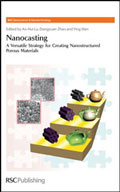


Nanocasting: A Versatile Strategy for Creating Nanostructured Porous Materials
An-Hui Lu, Dalian University of Technology, China Dongyuan Zhao, Fudan University, China Ying Wan, Shanghai Normal University, China
This book focuses on the synthesis of porous solids and introduces nanocasting from fundamental principles to their use in the synthesis of various materials. Special attention is given to new developments in this field and future perspectives and topics covered include inorganic chemistry, organic chemistry, solution chemistry, sol-gel and interface science, acid-base equilibria, electrochemistry, biochemistry and confined synthesis.


Unravelling Single Cell Genomics: Micro and Nanotools
Edited by Nathalie Bontoux, Agilent Technologies, France Maria-Claude Potier, CNRS France Luce Dauphinot, CNRS, France

This unique introduction to the growing field of microfluidics applied to genomics provides an overview of the latest technologies and emphasizes its potential in answering important biological questions. Aimed predominantly at graduate students, this book provides all the necessary information to conduct experiments in microfluidics and molecular biology.
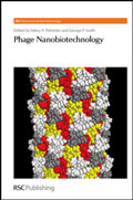


Phage Bionanotechnology
Edited by Valery Petrenko, Auburn University, USA George Smith, University of Missouri, USA

Recently, phage - as a new kind of nanomaterial has attracted attention of specialists working in the boundaries of the field and even further afield from genetics and molecular biology, such as pharmaceutical science, material science, microelectronics, biosensors, detection, environmental sciences, etc. This comprehensive book, of value to researchers in all fields, brings the phage display technique closer to specialists in areas of medicine, science and technology, where phage-derived nanomaterials can be most beneficial.
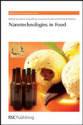

Nanotechnologies in Food
Edited by Qasim Chaudhry, Laurence Castle, Richard Watkins, DEFRA Central Science Laboratory, UK

This book provides a source of much needed and up-to-date information on nano foods and food contact materials. Ideal for scientists, regulators, industrialists and consumers alike, this valuable book reviews current developments in the field and highlights areas of uncertainty in relation to safety of the consumer and the environment, and regulatory inadequacies and gaps. The authors provide a balanced and impartial view of the applications of the new technology in food and food packaging, as well as addressing broader consumer safety and regulatory issues.


Bionanodesign: Following Nature's Touch
Maxim Ryadnov, National Physical Laboratory, UK

Bionanodesigns are improving our understanding of biomolecular folding and structure. This practical guide to molecular nanotechnology describes the concept of, and provides rules for, building nanostructures from basics. It is, in essence, a fully referenced review, placed in the context of de novo biomolecular design. Illustrations and references provide an essential support to the text and a special appendix lists "who's who in nanodesign". This comprehensive publication brings together contemporary approaches for designing nanostructures that employ naturally derived self-assembling motifs as synthetic platforms.

“Ryadnov’s review of bioinspired nanomaterials is a timely contribution to this fast-paced field.” Reviewed in Journal of the American Chemical Society


Nanoscale

A new peer reviewed journal publishing experimental and theoretical work across the breath of nanoscience and nanotechnology.


Lab on a Chip

Microfluidic & nanofluidic technologies for chemistry, physics, biology and bioengineering.


For more information visit the website www.rsc.org/nanoscience today or email books@rsc.org This e-mail address is being protected from spambots. You need JavaScript enabled to view it for a full title listing.

Friday 11 February 2011

SMART SYSTEMS INTEGRATION 2011


European Conference & Exhibition
Dresden, Germany
22. - 23.03.2011

www.smartsystemsintegration.com


In over 60 lectures, 57 poster presentations and 5 keynote speeches sector experts from across the globe will inform about the latest developments, industrial applications and future trends.

Over 100 speakers and poster presenters from 19 countries present their latest research results and practical solutions at the SMART SYSTEMS INTEGRATION 2011 in oral and poster presentations. The special session by EPoSS, a tutorial on the subject of 3D Integration as well as a Special Session "Russia - Partner for Cooperation" complete the program.

Keynotes will be presented by:

· EPoSS
· European Commission
· CSEM
· Robert Bosch
· Tohoku University

The conference is supplemented by a Pre-Conference Field Trip, a Conference Dinner and a After Conference Field Trip. You will find detailed information in the conference program. The full descriptions of the presentations as well as the biographies of the speakers will be available mid of December. The special session by EPoSS is free of charge for all conference attendees, exhibitors and visitors.

The concurrent exhibition is the right place for research institutions, manufacturers, suppliers, service providers, producers of sub-assemblies, components and systems in the sectors microsystems and nanotechnology, microelectronics, micromechanics, sensor technology and wireless communication.


Technology - Smaller! Smarter! Integrated!
Smart Systems Integration allows you to form a system out of components which is able to gain information from the environment, to process it electronically, to communicate signals and data and to give enabled feedback signal to the ambience.

The whole system is subject to the trend of today’s world: miniaturization, networking capability, energy-autonomy and reliability. Due to increasing complexity and multidisciplinarity developing teams in fields of microsystems- and nanotechnology, optics, fluidics, biology, medical science, electronics and wireless communication technologies face highest demands.

The conference gives a comprehensive overview about the latest developments, applications and possibilities as well as trends and visions.

Early bird prices are available until 18 February 2011

To learn more about SMART SYSTEMS INTEGRATION 2011 please contact:

Rebecca Zondler, Project Manager
Phone +49 711 61946-16
Fax +49 711 61946-90
Rebecca.Zondler@mesago.com


Or General inquiry:
Mesago Messe Frankfurt GmbH
Rotebuehlstr. 83-85, 70178 Stuttgart, Germany
Phone +49 711 61946-0
Fax +49 711 61946-90

Register as a delegate at: www.smartsystemsintegration.com/registration

Conference program -> www.smartsystemsintegration.com/program

Exhibitor list -> www.smartsystemsintegration.com/exhibitorlist